- 您现在的位置:买卖IC网 > Sheet目录345 > N08L63W2AB27I (ON Semiconductor)IC SRAM 4MBIT 70NS 48BGA
N08L63W2A
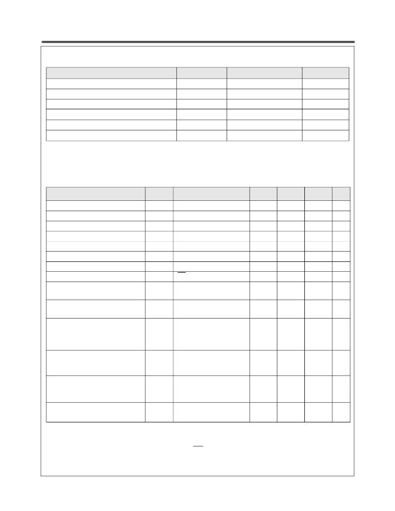
Absolute Maximum Ratings 1
Item
Voltage on any pin relative to V SS
Voltage on V CC Supply Relative to V SS
Power Dissipation
Storage Temperature
Operating Temperature
Soldering Temperature and Time
Symbol
V IN,OUT
V CC
P D
T STG
T A
T SOLDER
Rating
–0.3 to V CC +0.3
–0.3 to 4.5
500
–40 to 125
-40 to +85
260 o C, 10sec
Unit
V
V
mW
o C
o C
o C
1. Stresses greater than those listed above may cause permanent damage to the device. This is a stress rating only and functional
operation of the device at these or any other conditions above those indicated in the operating section of this specification is not
implied. Exposure to absolute maximum rating conditions for extended periods may affect reliability.
Operating Characteristics (Over Specified Temperature Range)
Item
Supply Voltage
Data Retention Voltage
Input High Voltage
Input Low Voltage
Symbol
V CC
V DR
V IH
V IL
Test Conditions
3
Chip Disabled
Min.
2.3
1.8
1.8
–0.3
Typ 1
3.0
Max
3.6
V CC +0.3
0.6
Unit
V
V
V
V
Output High Voltage
Output Low Voltage
Input Leakage Current
Output Leakage Current
V OH
V OL
I LI
I LO
I OH = 0.2mA
I OL = -0.2mA
V IN = 0 to V CC
OE = V IH or Chip Disabled
V CC –0.2
0.2
0.5
0.5
V
V
μ A
μ A
Read/Write Operating Supply Current
@ 1 μ s Cycle Time 2
Read/Write Operating Supply Current
@ 70 ns Cycle Time 2
I CC1
I CC2
V CC =3.6 V, V IN =V IH or V IL
Chip Enabled, I OUT = 0
V CC =3.6 V, V IN =V IH or V IL
Chip Enabled, I OUT = 0
2.0
9.0
3.0
15.0
mA
mA
Page Mode Operating Supply Current
@ 70ns Cycle Time 2 (Refer to Power
Savings with Page Mode Operation
I CC3
V CC =3.6 V, V IN =V IH or V IL
Chip Enabled, I OUT = 0
2.0
3.0
mA
diagram)
Read/Write Quiescent Operating Sup-
ply Current 3
I CC4
V CC =3.6 V, V IN =V IH or V IL
Chip Enabled, I OUT = 0,
f=0
3.0
mA
V IN = V CC or 0V
Maximum Standby Current 3
Maximum Data Retention Current 3
I SB1
I DR
Chip Disabled
t A = 85 o C, V CC = 3.6 V
Vcc = 1.8V, V IN = V CC or 0
Chip Disabled, t A = 85 o C
4.0
20.0
10
μ A
μ A
1. Typical values are measured at Vcc=Vcc Typ., T A =25°C and not 100% tested.
2. This parameter is specified with the outputs disabled to avoid external loading effects. The user must add current required to drive
output capacitance expected in the actual system.
3. This device assumes a standby mode if the chip is disabled (CE1 high or CE2 low). In order to achieve low standby current all
inputs must be within 0.2 volts of either VCC or VSS.
Rev. 8 | Page 3 of 10 | www.onsemi.com
发布紧急采购,3分钟左右您将得到回复。
相关PDF资料
N1JP1212
PANEL INNER 10.25X10.25" GREY
N252-012
PANEL PATCH CAT6 568B 12PORT
N252-024
PANEL PATCH CAT6 568B 24PORT
N252-048
PANEL PATCH CAT6 RACK 48 PORT
N25S818HAS21I
IC SRAM 256KBIT 16MHZ 8SOIC
N25S830HAS22IT
IC SRAM 3V SER 256KB LP 8SOIC
N64S818HAT21I
IC SRAM 64KB 1.8V LP 8-TSSOP
N64S830HAT22I
IC SRAM 64KBIT 20MHZ 8TSSOP
相关代理商/技术参数
N08L63W2AB27IT
制造商:ONSEMI 制造商全称:ON Semiconductor 功能描述:8Mb Ultra-Low Power Asynchronous CMOS SRAM 512K × 16 bit
N08L63W2AB7I
功能描述:静态随机存取存储器 8MB 3V LOW PWR 静态随机存取存储器 RoHS:否 制造商:Cypress Semiconductor 存储容量:16 Mbit 组织:1 M x 16 访问时间:55 ns 电源电压-最大:3.6 V 电源电压-最小:2.2 V 最大工作电流:22 uA 最大工作温度:+ 85 C 最小工作温度:- 40 C 安装风格:SMD/SMT 封装 / 箱体:TSOP-48 封装:Tray
N08L63W2AB7IT
制造商:ONSEMI 制造商全称:ON Semiconductor 功能描述:8Mb Ultra-Low Power Asynchronous CMOS SRAM 512K × 16 bit
N08M1618L1A
制造商:AMI 制造商全称:AMI 功能描述:8Mb Ultra-Low Power Asynchronous Medical CMOS SRAM 512K 】 16 bit
N08M1618L1AB
制造商:AMI 制造商全称:AMI 功能描述:8Mb Ultra-Low Power Asynchronous Medical CMOS SRAM 512K 】 16 bit
N08M1618L1AW
制造商:AMI 制造商全称:AMI 功能描述:8Mb Ultra-Low Power Asynchronous Medical CMOS SRAM 512K 】 16 bit
N08M163WL1A
制造商:NANOAMP 制造商全称:NANOAMP 功能描述:8Mb Ultra-Low Power Asynchronous Medical CMOS SRAM 512Kx16 bit
N08M163WL1AB
制造商:NANOAMP 制造商全称:NANOAMP 功能描述:8Mb Ultra-Low Power Asynchronous Medical CMOS SRAM 512Kx16 bit
